- No products in the cart.


Top 4 Methods to Inspect Wafers

Jun
13
2020
Due to the advancement in science, more and more gadgets and systems are being developed. As the number of tech tools increase, it becomes difficult to inspect them on a regular basis. The process of producing silicon wafers and chips is facing a similar fate.
Even with the best inspection tools and guidelines in place, detecting up to 30 nanometer defects in silicon wafers may still prove difficult.
However, chipmakers can rely on the following effective wafer inspection methods to identify common un-patterned defects.

- Electron-Beam Inspection
Although electron-beam inspection is mainly used for engineering analysis, it is also the first line of defense against small defects. The method involves using a highly focused beam to look for the tiniest of all defects in a silicon wafer.
If used properly, the e-beam can trace defects of up to three nanometers. However, e-beams offer a very slow throughput. So if you want to speed up the wafer production and inspection process, using e-beams may not be a good idea.
- Brightfield Inspection
Brightfield inspection uses 193 nanometer light sources, and it is one of the best ways to spot various defects in wafers. The technology works by collecting the light that reflects from a defect, and the defect then appears as a dark spot against a white background.
Brightfield inspection can easily trace defects of up to 30 nanometers. However, the method may not prove effective in detecting defects that range between 10 to 20 nanometers. Scientists are currently working on improving the brightfield method to identify the smallest possible defects.
- Multi-Beam Inspection
The multi-beam inspection was introduced as a way to overcome the slow throughput of the e-beam detection method. However, multi-beam inspection will not entirely eliminate e-beam and optical wafer inspection methods.
One of the limitations of multi-beam inspection is that it uses various beams with different electrons. If these electrons collide with each other, it could impact the overall performance and efficiency of this inspection method.

- Darkfield Inspection
Like the brightfield inspection method, darkfield is an optical technology. It simply measures the light reflected at a lower angle.
Other Detection Tools
In addition to the wafer inspection methods mentioned earlier, several types of equipment can be used to identify and correct the smallest possible defects. Some of the most widely used industrial systems include:
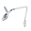
- VIZOR-A - VISUAL INSPECTION SYSTEM:The new ergonomic, stereo, visual inspection system from Scienscope. Inspect with accuracy and work in comfort without eyepieces. This System is affordably priced with several lenses including 4x, 6x and 8x. The Vizor-A model comes with a sturdy articulating arm stand and c-clamp.
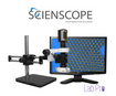
- EMZ-5 (0.7x - 4.5x) Binocular Greenough Design, Stereo Zoom Body:The EMZ-5 body delivers sharp, high-contrast images and an excellent zoom range of 6.5:1 that provides exceptionally high-resolution images all throughout the zoom range. The EMZ-5 employs Greenough optics, for improved image flatness and contrast. As a result, images are brighter and more distinct even at the periphery of the field of view. With the large zoom range, the EMZ-5 offers high resolution observation in precision-oriented semi-conductor, medical device and routine inspection. In addition to its compact design and versatility a wide variety of auxiliary lenses and stands are available to allow the user to customize their desired working distance to adapt to almost any application.
- The NZ Stereo Zoom Trinocular Microscope is designed for all industrial, electronic, and medical manufacturing applications. It boasts a new, rugged, air and moisture tight housing, and unbreakable eyepiece ports. It is perfect for the rigors of the assembly line or any harsh manufacturing environment. This also make s the NZ virtually maintenance free.a
Whether you need help inspecting silicon wafers or a high-quality system that identifies detects at high throughputs, get in touch with a Lab Pro experts today!